Chapter 8: Solid-State Physics
This chapter provides a fundamenal introduction to Solid State Physics, tailored for undergraduae students in Chemistry, Physics, and Engineering. Building upon a basic understanding of University Physics, Quantum Mechanics and Statistical Mechanics, this chapter explore the essential concepts underlying the structure and electronic properties of materials. To enhance comprehension, the chapter incorporates various simulation that visulize key concepts and provide hands-on experience with programming.
11.1 Introduction
In crystalline solids, atoms are arranged in a periodic array, forming a highly ordered structure that repeats throughout the material. These atoms are held together by various types of bonding interactions, which determine the solid’s properties.
Our goal is to understand the properties of materials from a microscopic perspective. To achieve this, we first need to grasp the terminology used to describe the microscopic structure of materials that exhibit periodicity.
In this chapter, we will explore the crystalline structure of materials by first examining one-dimensional examples in detail. This approach allows us to build a foundational understanding of periodic structures and their properties in a simplified context. Once we establish these concepts, we will extend our study to three-dimensional structures, where we will examine more complex and realistic crystal arrangements found in actual materials.
11.2 One-Dimensional Periodic Structures
A one-dimensional lattice is an infinite array of points arranged along a line, where each point is separated by a constant distance.
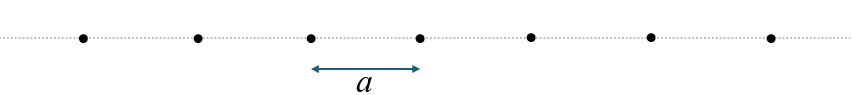
The black dots in the diagram represent lattice points. In a hypothetical one-dimensional crystalline system, an atom or a group of atoms repeats at regular intervals, defined by the lattice constant, just as the dots repeat along the line.
With this example, let’s explore the terminology commonly used in crystalline systems.
The Figure 2 shows the …
Lattice Constant: A fundamental parameter of a crystal structure, It defines the periodicity and spacing of the atoms within the lattice.
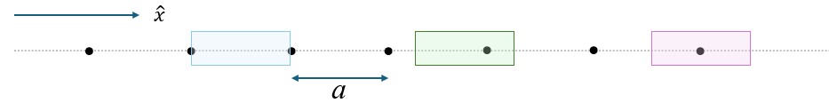
Lattice Translation Vector: The lattice translation vector is a vector that describes the displacement needed to move from one lattice point to another in a crystal lattice, such that the structure remains unchanged. It defines the periodicity of the crystal.
For the above 1-Dimensional system:
\begin{equation} \vec{T} = a \hat{x} \tag{11.1} \end{equation}
Primitive Unit Cell: A primitive unit cell is the smallest repeating unit in a crystal lattice that, when translated through space, can recreate the entire crystal structure without any gaps or overlaps. It contains exactly one lattice point (or an equivalent portion of lattice points) and captures the symmetry and periodicity of the crystal.
The Primitive Unit Cell is not unique For example, all three boxes shown in blue, purple and green in the Figure-xx represent primitive unit cells for this configuration.
Basis : The basis refers to the atom or group of atoms associated with each lattice point. In a 1D crystal, the basis could be a single atom or a repeating group of atoms that accompanies each lattice point, creating a consistent pattern along the line.
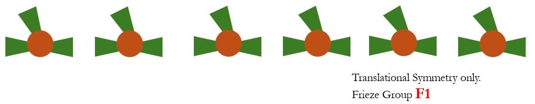
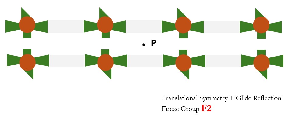
11.2.1 Symmetry in 1-Dimensional Crystals and Frieze groups
A one-dimensional crystal has translational symmetry, meaning it looks the same if shifted by an integer multiple of the lattice constant \(a\).
In some cases, additional symmetry operations. In a one-dimensional (1D) crystal, symmetry refers to the transformations that can be applied to the crystal structure such that the arrangement appears unchanged.
- Translational Symmetry: Frieze Group F1 Translational symmetry is the most fundamental form of symmetry. In 1D, if you shift the entire structure along the line by an integer multiple of the lattice constant, the arrangement of points or
- Translational Symmetry + 1800 (2-fold) rotation about a point P: Frieze Group F2
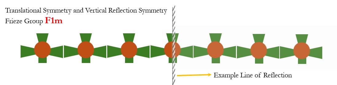
- Translational Symmetry and Vertical Reflection Symmetry: Frieze Group F1m. The structure remains unchanged if it is reflected across a vertical line (a mirror line) positioned at specific points along the line.
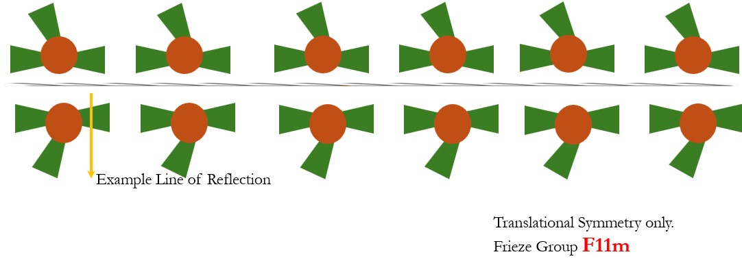
- Translational Symmetry and Horizontal Reflection Symmetry: Frieze Group F11m. The structure remains unchanged if it is reflected across a vertical line (a mirror line) positioned at specific points along the line.
- Translational Symmetry 2-fold Rotation + Vertical Reflection Symmetry + Horizontal Reflection Symmetry : Frieze Group F2mm. The structure remains unchanged if it is reflected across a vertical line (a mirror line) positioned at specific points along the line.

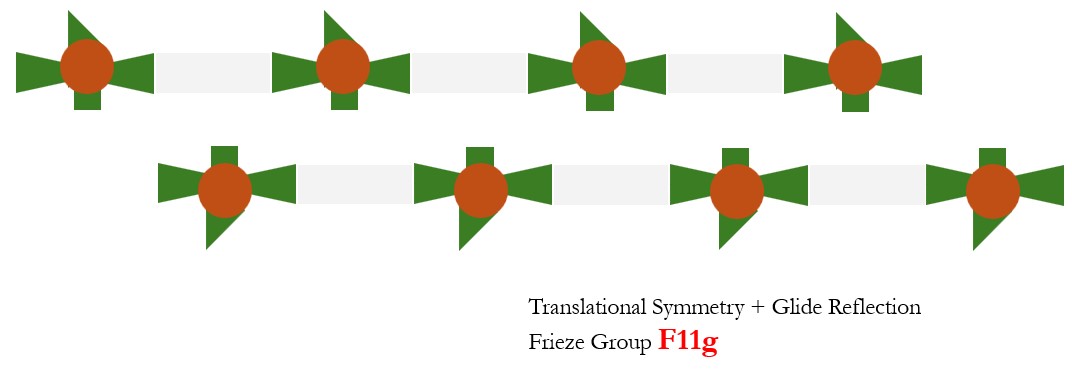
- Translational and Glide Reflection: Frieze Group F11g. A glide reflection involves reflecting the structure across a line, followed by a translation by half the lattice constant. This symmetry operation can repeat the pattern in a 1D crystal.
11.2.2 Symmetry in 2-Dimensional Crystals and Plane Groups and 2D Bravais Lattices
In 2-DImensions, an infinite array of lattice points can be described bythe translational vector:
\[\begin{equation} \vec{T}=n \vec{a}_1 + m \vec{a}_2 \tag{11.2} \end{equation}\]11.2.3 Symmetry in 3-Dimensional Crystals and Space groups and 3D Bravais Lattices
11.3 Electron Materials
Electrons are negatively charged particles, which are the key carriers of electrical current. The behavior of electrons in materials is fundamental to understanding the properties of matter. Electrons in materials behave quite different from those free electrons. Such differences give rise to materials with variety of phenomena with varying electrical conductivity, magnetism, optics, and thermal properties. It is our goal to study the properties of electron materials.
11.3.1 Classsical Theory of Electron- Drude Model
The Drude model treats electrons in a metal as a gas of classical, free particles that move randomly and occasionally collide with fixed ions, leading to resistive behavior. This model successfully explains electrical conductivity. But Drude model cannot explain some other electronic properties of materials as we will explain later.
Basic assumptions of Drude model are:
- Electrons in a solid behave like a classical ideal gas with no interactions or collisions between them.
- Electrons move freely but occasionally collide with fixed ion cores, changing their speed.
- Electrons react equilibrium : \(\begin{equation} \frac{1}{2} m v_t ^2 = \frac{3}{2} k_B T \tag{11.3} \end{equation}\)
At room temperature \(v_t = 10^5 m/s\)
- In between collisions, electrons move freely. The average length electrons travel in between collisions is called electron mean free path \(\lambda\). That relates to the relaxation time as \(\tau = \lambda/v_t\)
Using these assumptions, we can calculate the electronic properties based on classical theory, which align well with the observed behavior of electrons in metals.
11.3.2 DC Electrical Conductivity
Let’s apply the Newton’s equation of motion for the electron motion in an electric field.
\[\begin{eqnarray} \vec{F} &=& -e \vec{E} \nonumber \\ m_e \frac{d\vec{v}}{dt} &=& -e \vec{E} \nonumber \\ \vec{v}(t) &=& - \frac{e}{m} \vec{E} t \tag{11.4} \end{eqnarray}\]Assuming that the kinetic energy pf electrons is lost during collisions with ions, and the average time between collisions (relaxation time \(\tau\)),
the average drift velocity of electrons is:
\[\begin{equation} \vec{v}_d= - \left(\frac{e}{m} \right) \vec{E} \tau \tag{11.5} \end{equation}\]Now let’s consider a conducting wire with a cross section area \(A\):
The electrons travel through \(A\) per unit time is:
\[\begin{equation*} n v_d A \end{equation*}\]That is, we can write the electric current density across the conductor as
\[\begin{equation} \vec{J}=-e n \vec{v}_d \tag{11.6} \end{equation}\]By substituting for \(\vec{v}_d\), we get:
\[\begin{eqnarray} \vec{J}=-e n \left(- \frac{e}{m} \vec{E} \right)\tau \nonumber \\ \vec{J}= \left(\frac{n e^2 \tau }{m_e} \right) \vec{E} \tag{11.7} \end{eqnarray}\]The current is in the direction of the $\vec{E}$ field and is proportional to the strength of the electric field.
The proportionality constant is the electrical conductivity, \(\sigma\)
\[\begin{equation} \sigma =\frac{n e^2 \tau }{m_e} \tag{11.8} \end{equation}\]Limitations of Drude’s Model for Electron Conductivity
11.3.3 Quantum Mechanical Approach for Electrons
Let’s assume that electrons are not classical particle, instead they behave according to \(\begin{equation} H\Psi = E\Psi \tag{11.9} \end{equation}\)
This gives rise to electron energy levels:
\[\begin{equation} E_n =\frac{\hbar ^2 }{2 m_e } (k_x^2 + k_y^2 +k_z^2) \tag{11.10} \end{equation}\]With the periodic boundary conditions \(k_x=\left(2\pi/L\right) n_x\), we get
\[\begin{eqnarray} E_n &=&\frac{\hbar ^2 }{2 m_e } \left(\frac{2\pi}{L}\right)^2 (n_x^2 + n_y^2 +n_z^2) \nonumber \\ &=& \left(\frac{2 \pi ^2 \hbar^2 }{m_e L^2 } \right) n^2 \tag{11.11} \end{eqnarray}\]The total number of states:
\[\begin{equation} N=\frac{1}{(2\pi/L)^3 4 \pi k^2 dk} \tag{11.12} \end{equation}\]With this, we get the DoS as
\[\begin{equation} g(E)=\frac{V}{2\pi^2} \left( \frac{2 m_e}{\hbar^2 } \right)^{3/2} E^{\frac{1}{2}} \tag{11.13} \end{equation}\]If we want to calculate the total number of available states, we can find it as :
\[\begin{equation*} \int_{E_{min}}^{E_{max}} g(E) dE \end{equation*}\]However, our goal is not to calculate the number of states, but rather to determine the total number of available electrons within a specific energy range. To do this, we must consider whether the states are occupied.
That for example give total number of electrons as:
\[\begin{equation} n=\int_{E_{min}}^{E_{max}} f(E) g(E) dE \tag{11.14} \end{equation}\]where \(f(E)\) is the Fermi Dirac Distribution function.
11.3.4 Fermi Dirac Distribution function
The Fermi-Dirac distribution function describes the probability that a quantum state with energy \(E\) is occupied by a fermion (such as an electron) at a given temperature \(T\). It accounts for the Pauli Exclusion Principle, allowing at most one fermion per quantum state.
Fermi Dirac function is proven by statistical mechanics to satisfy the above conditions.
\[\begin{equation} f(E)=\frac{1}{e^{(E-E_F)/k_BT}+1} \tag{11.15} \end{equation}\]where \(E_F\) is the Fermi energy, \(k_B\) is the Boltzmann constant, and \(T\) is the absolute temperature.
At absolute zero, states below \(E_F\) are fully occupied, and those above are empty. At higher temperatures, states near \(E_F\) have fractional occupancy due to thermal excitations.
The Fermi-Dirac function can be plotted for different temperatures to illustrate how the occupation probability of energy states changes with temperature.
At \(0 K\), all states with energies below the Fermi energy (\(E_F\)) are fully occupied, while those above are empty. As temperature increases, the Fermi-Dirac distribution changes, causing some states below \(E_F\) to excite to levels higher than \(E_F\).
The Fermi wave vector \(k_F\) of the electrons at \(E=E_F\) is given by:
\[\begin{eqnarray} E_F&=&\frac{\hbar ^2 k_F^2}{2m_e} \nonumber \\ k_F &=& \sqrt{2 m_e E_F}/\hbar \tag{11.16} \end{eqnarray}\]11.3.5 Fermi Wave vector and Electron Concentration
from \(\begin{eqnarray} 2 \frac{1}{(2\pi/L)^3} \frac{4}{3} \pi k_F ^3 &=& N \nonumber \\ k_F &=& \left(\frac{3 \pi ^2 N}{V}\right)^{1/3} \tag{11.17} \end{eqnarray}\)
\[\begin{equation} E_F = \frac{\hbar^2}{2m} \left(\frac{3 \pi ^2 N}{V}\right)^{2/3} \tag{11.18} \label{eq:11-18} \end{equation}\]Just Checking Back:
\[\begin{equation*} \int_0 ^\infty f(E)g(E)dE = \int_0 ^{E_{F}} g(E)dE \end{equation*}\]We used absolute zero temperature conditions:
\[\begin{eqnarray} &=& \int_0 ^{E_F}\frac{V}{2\pi^2} \left( \frac{2 m_e}{\hbar^2 } \right)^{3/2} E^{\frac{1}{2}} dE \nonumber \\ &=& \frac{V}{2\pi^2} \left( \frac{2 m_e}{\hbar^2 } \right)^{3/2} \int _0 ^{E_F} E^{\frac{1}{2}} dE$ \nonumber \\ &=& \frac{V}{2\pi^2} \left( \frac{2 m_e}{\hbar^2 } \right)^{3/2} \frac{2}{3} E_F^{3/2} \tag{11.19} \end{eqnarray}\]By substituting from Eq. \ref{eq:11-18}:
$$ \begin{equation} N = \frac{V}{2\pi^2} \left( \frac{2 m_e}{\hbar^2 } \right)^{3/2} \frac{2}{3} \left( \frac{\hbar^2}{2m_e} \right)^{3/2} \left(\frac{3 \pi ^2 N}{V}\right) \tag{11.20} \end{equation}
We just proved \(\int_0 ^\infty f(E) g(E) dE = N\) at zero temperature conditions.
11.4 Formation of Bands
In the earlier discussion, electrons were treated as free particles. Now, we consider the influence of the periodic arrangement of the crystalline lattice.
When the electrons belong to a single atom, they are localized around the nucleus. The wave function can be represented as follows.
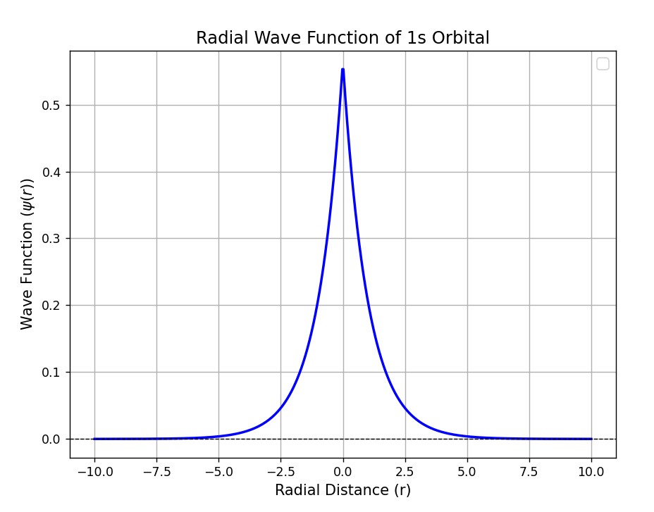
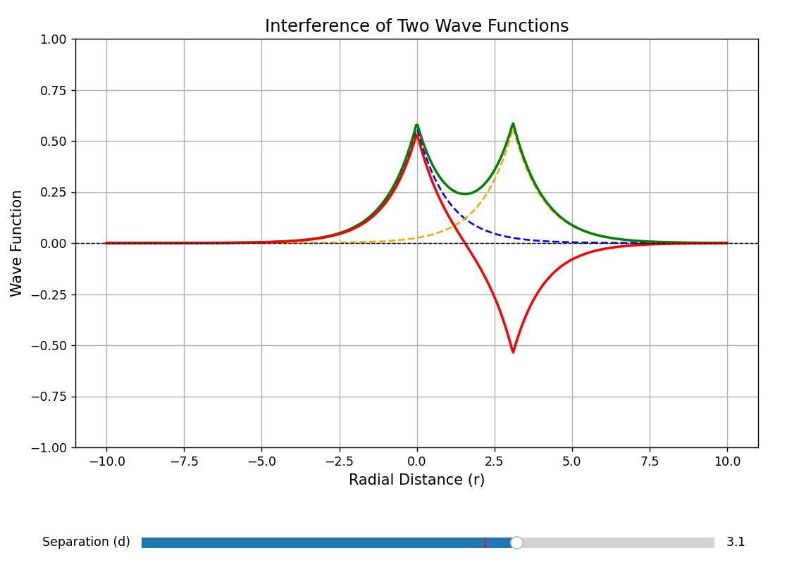
Let’s consider the wave function of electrons in a 2 atomic system. The wave function of the composite system can be written as a linear combination of the individual atomic systems.
The two wave functions can be written as
\[\begin{equation} \Psi_+ = \Psi_1 (r) + \Psi_2 (r) \tag{11.21} \end{equation}\]and
\[\begin{equation} \Psi_- = \Psi_1 (r) - \Psi_2 (r) \tag{11.22} \end{equation}\]The \(\Psi_+\) is represented by the green line, and the \(\Psi_-\) is depicted by the red line. \(\Psi_+\) indicates a higher probability of finding electrons at the center between the atoms. As the atoms come closer together, the 1s orbitals split into two distinct energy levels. With an increasing number of atoms, additional energy levels emerge from various linear combinations of atomic orbitals, forming a dense set of closely spaced levels known as energy bands.
The characteristics of these energy bands significantly influence the material’s electronic properties, leading to behaviors ranging from metallic to semiconducting or insulating, depending on the nature of the band formation.
The lower energy bands are fully occupied. At absolute zero, the highest occupied energy level is referred to as the Fermi level, as previously discussed in the free electron model. The occupation probability as a function of temperature is described by the Fermi-Dirac distribution function as proven in the section on Statistical physics.
The position of the Fermi level relative to the lowest unoccupied energy level plays a crucial role in determining how the material responds to an external electric field.
In metals, the Fermi level lies within the middle of overlapping energy bands, meaning there is no gap between the highest occupied and lowest unoccupied levels at zero temperature.
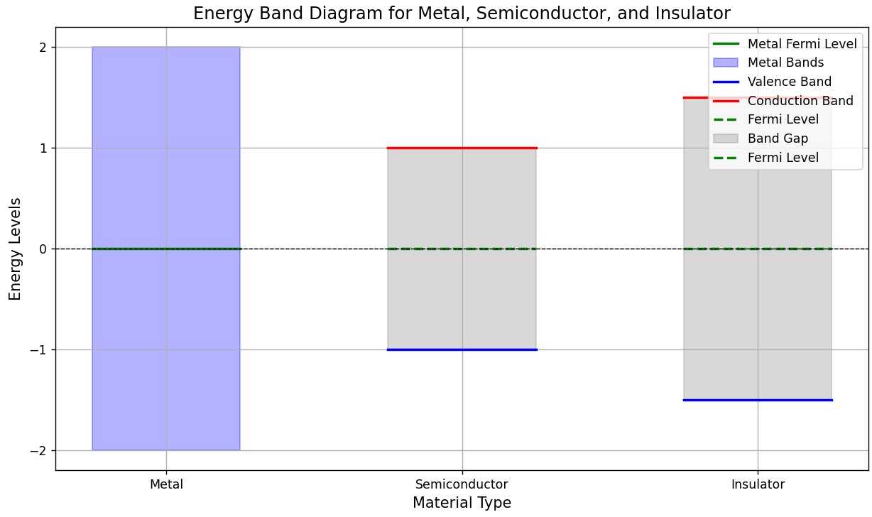
- The valence band is the highest energy band that is fully occupied with electrons at absolute zero temperature, while the conduction band is the next higher energy band, which is typically empty at absolute zero.
- The Fermi level is the energy level at which the probability of occupation is 50%, separating the filled states from the empty states at zero temperature.
When a gap exists between the highest occupied and lowest unoccupied levels, the material’s response to an electric field depends on the size of the gap. If the gap is large enough that no significant number of electrons can be thermally excited into the conduction band, the material cannot conduct electricity and behaves as an insulator.
However, if the gap is smaller, increasing the temperature allows a notable number of electrons to be excited from the valence band to the conduction band, enabling electrical conductivity. Materials that behave in this way are known as semiconductors.
11.5 Semiconductors
Semiconducting materials have an electron band gap typically below 4 eV. While the band gap may change with temperature, we will ignore this temperature dependence in this discussion.
The following table presents the reported electron band gaps for several semiconducting materials.
Table 1: Reported Electron Band Gaps for Semiconducting Materials
| Material | Band Gap (eV) |
|---|---|
| Silicon (Si) | 1.12 |
| Germanium (Ge) | 0.66 |
| Gallium Arsenide (GaAs) | 1.43 |
| Silicon Carbide (SiC) | 3.26 |
| Gallium Nitride (GaN) | 3.4 |
| Zinc Oxide (ZnO) | 3.37 |
| Cadmium Telluride (CdTe) | 1.44 |
| Indium Phosphide (InP) | 1.34 |
At 0K, the valance band is completely filled in a semiconductor. As temperature increases, more and more thermally excited carriers are available such that conductivity increases as the temperature increases.
11.6 Charge Carriers in Semiconductors
It is clear from the above discussion that electrons thermally excited to conduction band are current carriers.
When the electrons are excited, they leave bhehind an empty sttae in the valance band. These vacant states are called holes.